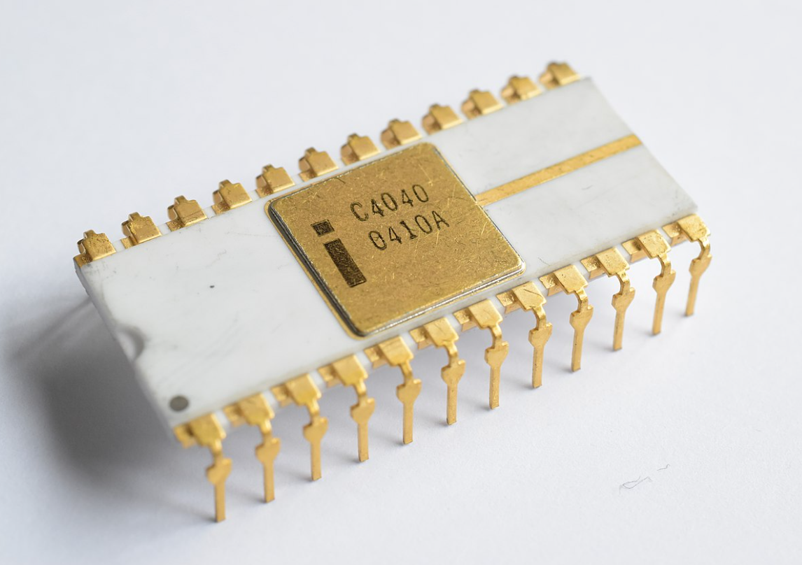
인텔 4040(“포티-포티”)는 인텔이 설계하고 제조한 두 번째 4비트 마이크로프로세서로, 1974년에 인텔 4004의 후속 제품으로 출시되었다. 이 프로세서는 10μm 공정으로 제작되었으며, 실리콘 게이트 강화 로드 PMOS 논리 기술을 포함하고 있다. 4040은 3,000개의 트랜지스터를 포함하고 있으며, 초당 약 62,000개의 명령어를 실행할 수 있다.
일반 성능, 버스 레이아웃 및 산술 논리 유닛(ALU)은 4004와 동일하지만, 주요 개선 사항은 16핀 4004보다 8핀 더 많은 24핀 듀얼 인라인 패키지를 사용한 것이다. 이 추가 핀 중 두 개는 인터럽트를 구현하는 데 사용되어 4004의 큰 결점으로 여겨졌던 점을 보완했다. 또 다른 두 개는 프로세서를 저전력 모드로 전환하는 정지/정지 시스템을 구현하여 디버깅을 훨씬 쉽게 했다. 하나의 핀은 두 번째 읽기 전용 메모리(ROM)를 선택할 수 있도록 해주어, 4004와 비교해 프로세서가 주소할 수 있는 ROM의 양을 두 배로 늘렸다.
이 새로운 핀을 활용하기 위해 명령어 집합이 확장되어 46개에서 60개로 증가했다. 또한 내부 레지스터 파일과 푸시다운 스택이 확장되어 신속한 인터럽트 처리를 지원하게 되었다.
4040은 본질적으로 4004의 확장이며, 추가 핀, 더 많은 레지스터 및 새로운 명령어를 통해 이점을 극대화했다. 4004는 단일 ROM 핀을 가지고 있었으나, 4040은 두 개의 ROM 핀을 추가하여 두 개의 ROM 뱅크를 지원하게 되었다. 이로 인해 ROM 주소가 12비트에서 13비트로 증가하여 8KB를 지원하게 되었다.
4004는 인터럽트 기능이 부족했지만, 4040은 인터럽트를 호출하는 새로운 입력 핀과 인터럽트 신호가 인식되고 작동 중임을 나타내는 출력 핀을 추가했다. 인터럽트가 발생하면 반환 주소를 저장해야 하므로, 스택 레지스터 파일이 세 개에서 일곱 개로 확장되었다.
인터럽트 핸들러 코드는 보통 레지스터의 값을 저장한 후, 인터럽트 코드가 사용하도록 값을 메모리에서 복사하고 핸들러가 완료되면 원래 값을 복원하는 방식으로 진행된다. 이러한 설계를 통해 프로세서는 단일 명령어로 레지스터 은닉을 빠르게 처리하여 인터럽트 응답 시간을 크게 개선했다.
4040은 새로운 입력 정지 핀과 관련된 출력 정지 승인 핀을 추가하여, 시스템이 I/O 작업을 수행할 때 프로세서를 정지시키는 데 사용될 수 있었다. 이는 디버깅에서도 널리 사용되었으며, 프로세서를 단일 단계로 실행할 수 있게 했다. 정지 모드에 있을 때 대부분의 칩 하드웨어는 저전력, 고임피던스 상태로 전환되어 전력 소모가 줄어들었다.
이 새로운 기능을 활용하기 위해 명령어 집합은 14개의 새로운 명령어가 추가되어 총 60개로 늘어났다.
4040의 레지스터 구성은 누산기, 조건 코드, 인덱스 레지스터, 프로그램 카운터 및 푸시다운 주소 호출 스택으로 나뉜다. 데이터 버스는 4비트, 주소 버스는 ROM에 대해 12비트이며, 두 개의 뱅크 스위칭 명령을 통해 13비트로 확장되었다. 프로세서는 -15V DC 전압에서 작동하며, 주 클록 주파수는 500에서 740kHz로, 명령 실행은 보통 한 두 개의 기계 사이클을 필요로 하여 약 62 kIPS의 성능을 낸다.
4040의 설계자는 페데리코 파긴이었으며, 상세 설계는 톰 이네스가 담당했다. 이 프로세서와 함께 사용되는 새로운 지원 칩도 여러 개 출시되었고, 4040을 중심으로 한 최초의 마이크로컴퓨터인 마이크로 440은 1975년에 출시되었다.
The Intel 4040, also known as the "Forty-Forty," is Intel's second 4-bit microprocessor, released in 1974 as the successor to the Intel 4004. This processor was manufactured using a 10μm process and incorporated silicon gate enhanced load PMOS logic technology. The 4040 contains 3,000 transistors and can execute approximately 62,000 instructions per second.
While its general performance, bus layout, and arithmetic logic unit (ALU) are the same as the 4004, a major improvement is its use of a 24-pin dual in-line package, which has eight more pins than the 16-pin 4004. Two of these additional pins are used for implementing interrupts, addressing a significant flaw in the 4004. Another two pins enable a stop/hold system that allows the processor to switch to low-power mode, greatly facilitating debugging. One pin allows for the selection of a second read-only memory (ROM), effectively doubling the amount of ROM that can be addressed compared to the 4004.
To take advantage of these new pins, the instruction set was expanded from 46 to 60 instructions. Additionally, the internal register file and pushdown stack were enlarged to support fast interrupt handling.
The 4040 is essentially an extension of the 4004, maximizing benefits through additional pins, more registers, and new instructions. The 4004 had a single ROM pin, while the 4040 supports two ROM banks by adding two ROM pins. This increased the ROM address from 12 bits to 13 bits, allowing support for 8KB.
The 4004 lacked interrupt functionality, but the 4040 introduced new input pins for calling interrupts and output pins to indicate that an interrupt signal is recognized and in operation. When an interrupt occurs, the return address must be saved, so the stack register file was expanded from three to seven registers.
Interrupt handler code typically saves the values of registers, copies the values from memory for the interrupt code to use, and restores the original values once the handler completes. This design allows the processor to quickly handle register saving with a single instruction, significantly improving interrupt response times.
The 4040 added a new input stop pin and a related output stop acknowledge pin, which could be used to halt the processor during I/O operations. This was also widely used in debugging, allowing the processor to execute one step at a time. When in stop mode, most chip hardware transitions to a low-power, high-impedance state, reducing power consumption.
To utilize these new features, the instruction set was expanded to a total of 60 instructions with the addition of 14 new instructions.
The register configuration of the 4040 includes an accumulator, condition code, index register, program counter, and a pushdown address call stack. The data bus is 4 bits wide, and the address bus is 12 bits for ROM, expandable to 13 bits through two bank-switching commands. The processor operates at -15V DC and has a main clock frequency ranging from 500 to 740 kHz, with instruction execution typically requiring one or two machine cycles, resulting in a performance of approximately 62 kIPS.
The designer of the 4040 was Federico Faggin, with detailed design work done by Tom Innes. Several new support chips were released alongside this processor, and the first microcomputer centered around the 4040, the Micro 440, was launched in 1975.
インテル 4040(「フォーティ-フォーティ」)は、インテルが設計・製造した2番目の4ビットマイクロプロセッサで、1974年にインテル 4004の後継製品として発売されました。このプロセッサは10μmプロセスで製造され、シリコンゲート強化ロッドPMOS論理技術を取り入れています。4040は3,000個のトランジスタを含み、約62,000命令を毎秒実行できます。
一般的な性能、バスレイアウト、および算術論理ユニット(ALU)は4004と同じですが、主な改善点は、16ピンの4004より8ピン多い24ピンデュアルインラインパッケージを使用していることです。この追加された8ピンのうちの2つはインタラプトの実装に使われ、4004の大きな欠点を補っています。さらに2つはプロセッサを低消費電力モードに切り替えるストップ/ホールドシステムを実装し、デバッグが大幅に容易になりました。1つのピンは2番目の読み取り専用メモリ(ROM)を選択できるようにし、4004に比べてプロセッサがアドレスできるROMの量を2倍にしました。
これらの新しいピンを活用するために、命令セットは46から60命令に拡張されました。さらに、内部レジスタファイルとプッシュダウンスタックも拡張され、迅速なインタラプト処理がサポートされるようになりました。
4040は基本的に4004の拡張であり、追加ピン、より多くのレジスタ、そして新しい命令を通じて利点を最大化しました。4004は単一のROMピンを持っていましたが、4040は2つのROMピンを追加することで2つのROMバンクをサポートしました。これにより、ROMアドレスは12ビットから13ビットに増加し、8KBのサポートが可能になりました。
4004はインタラプト機能が不足していましたが、4040はインタラプトを呼び出すための新しい入力ピンと、インタラプト信号が認識されていることを示す出力ピンを追加しました。インタラプトが発生すると、戻りアドレスを保存する必要があるため、スタックレジスタファイルは3から7レジスタに拡張されました。
インタラプトハンドラーコードは通常、レジスタの値を保存し、インタラプトコードが使用するためにメモリから値をコピーし、ハンドラーが完了したら元の値を復元する方式で進行します。この設計により、プロセッサは単一の命令でレジスタ保存を迅速に処理でき、インタラプト応答時間を大幅に改善しました。
4040は新しい入力ストップピンと関連する出力ストップ承認ピンを追加し、I/O作業中にプロセッサを停止するために使用されました。これはデバッグでも広く使用され、プロセッサを1ステップずつ実行できるようになりました。ストップモードにあるとき、ほとんどのチップハードウェアは低消費電力、高インピーダンス状態に切り替わり、消費電力が減少しました。
これらの新機能を活用するために、命令セットは新たに14の命令を追加し、合計60命令になりました。
4040のレジスタ構成は、アキュムレータ、条件コード、インデックスレジスタ、プログラムカウンタ、およびプッシュダウンアドレス呼び出しスタックに分かれています。データバスは4ビット、ROMに対するアドレスバスは12ビットであり、2つのバンクスイッチングコマンドによって13ビットに拡張可能です。プロセッサは-15V DC電圧で動作し、主クロック周波数は500から740kHzの範囲で、命令実行には通常1または2の機械サイクルを必要とし、約62 kIPSの性能を発揮します。
4040の設計者はフェデリコ・ファギンであり、詳細な設計はトム・イネスが担当しました。このプロセッサと共に複数の新しいサポートチップも発売され、4040を中心にした最初のマイクロコンピュータであるマイクロ440は1975年に発売されました。
'Computer > CPU' 카테고리의 다른 글
| INTEL 8080 [INTEL / 1974] (0) | 2024.09.20 |
|---|---|
| INTEL 8008 [INTEL / 1972] (0) | 2024.09.19 |
| INTEL 4004 [INTEL / November 15, 1971] (0) | 2024.09.17 |
| IBM 701 [IBM / 1952] (0) | 2024.09.08 |